A Bright Future Ahead
Portable Spectral Services Announces Exciting Management Transition


Portable Spectral Services Announces Exciting Management Transition
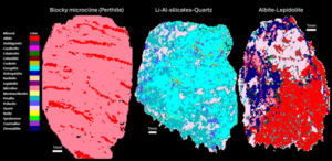
Our tool introduces uXRF (micro-X-ray fluorescence) scanning technology to RC chip analysis, enabling rapid, non-destructive, and quantitative analysis of major, minor, and trace mineral phases.
Automated micro-X-ray fluorescence (micro XRF) technology emerges as a powerful tool to rapidly and accurately capture the mineralogy of rock chip, RC and AC samples.

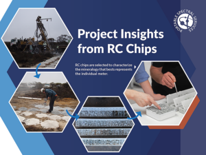
Findings of an ongoing regional evaluation study over concealed Proterozoic lithologies known to host magmatic nickel sulphides with potential to host other base-metal, gold and rare earth elements (“REE”) systems within the Fraser Range, Western Australia.
Findings of an ongoing regional evaluation study over concealed Proterozoic lithologies known to host magmatic nickel sulphides with potential to host other base-metal, gold and rare earth elements (“REE”) systems within the Fraser Range, Western Australia.

Findings of an ongoing regional evaluation study over concealed Proterozoic lithologies known to host magmatic nickel sulphides with potential to host other base-metal, gold and rare earth elements (“REE”) systems within the Fraser Range, Western Australia.